 PCB
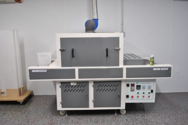
Panel Cutting Machine for PCB
Shears copper-clad laminate to panel size before drilling, with square edges for downstream registration.
- Panel up to 24 × 24 in
- CCL / FR-4 / CEM
- Square-cut, low burr
PCB process lines · wafer & chip tools
CNC and laser drilling, LDI, DES, plating, AOI and solder-mask lines for PCB. CZ furnaces, lithography, PVD, lapping and plasma etch for front-end chip work. Quoted against your process window.
Equipment range
Process equipment sourced for printed-circuit fabrication and front-end wafer / chip lines. Send panel size, wafer diameter and process window for a firm quote.
PCBShears copper-clad laminate to panel size before drilling, with square edges for downstream registration.
 PCB
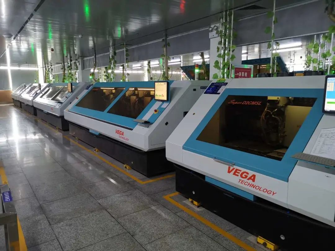
Multi-spindle CNC drilling for through-holes and tooling holes on rigid and multilayer panels.
 PCB
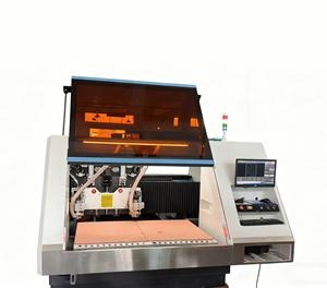
UV / CO2 laser microvia drilling for HDI and sequential-build-up boards.
 PCB
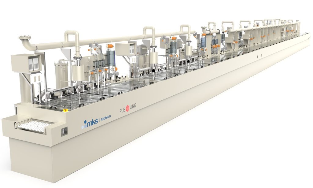
PTH line depositing seed copper in drilled holes before electrolytic plating.
 PCB
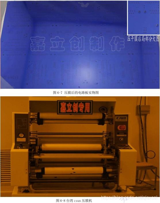
Hot-roll laminator applying photoresist dry film to cleaned copper surfaces.
 PCB
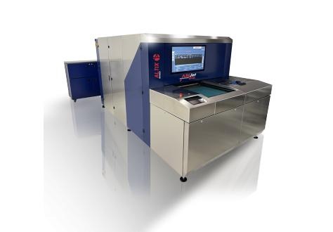
Maskless laser imaging of inner and outer layers, replacing film artwork.
 PCB
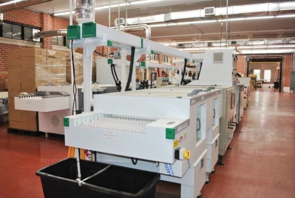
Horizontal wet line that develops, etches and strips dry film in one pass.
 PCB
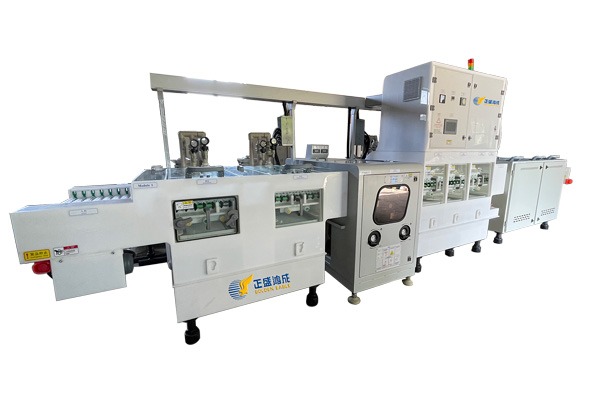
Camera AOI for inner layers, outer layers and solder mask before electrical test.
 PCB
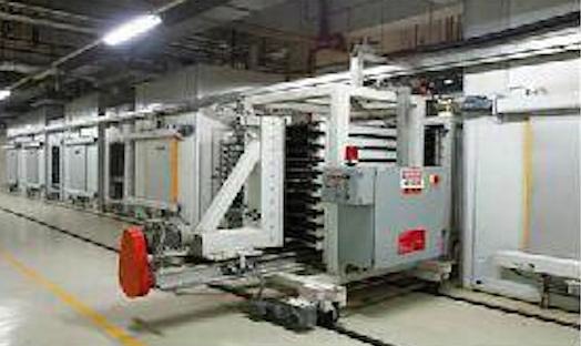
Multi-opening vacuum press bonding multilayer stacks with controlled heat and pressure.
 PCB
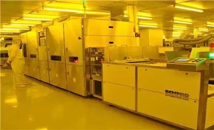
Screen or spray coating of liquid photoimageable solder mask onto outer layers.
 PCB
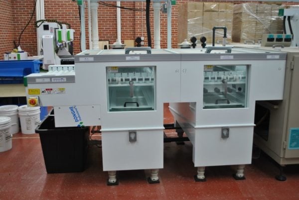
HASL / HAL finishing that coats exposed copper with solder and levels with hot air.
 PCB
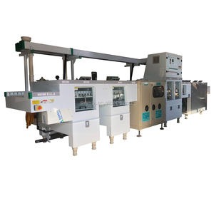
Mechanical brushing and chemical cleaning before dry-film lamination or solder mask.
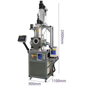 CHIP
Czochralski furnace growing monocrystalline silicon ingots for wafer starting material.
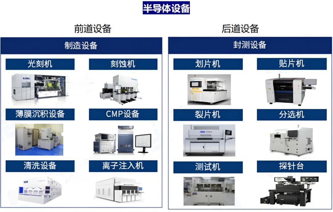 CHIP
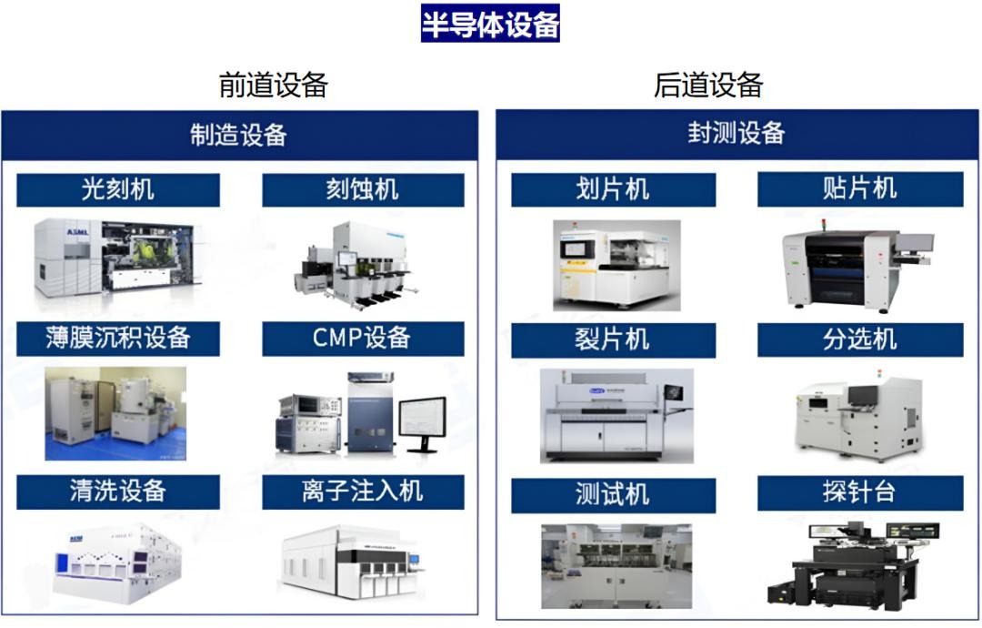
Grouped core tools for front-end wafer lines: clean handling, process modules and metrology interfaces.
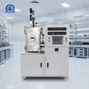 CHIP
Magnetron sputter tool depositing metal and barrier films on wafers.
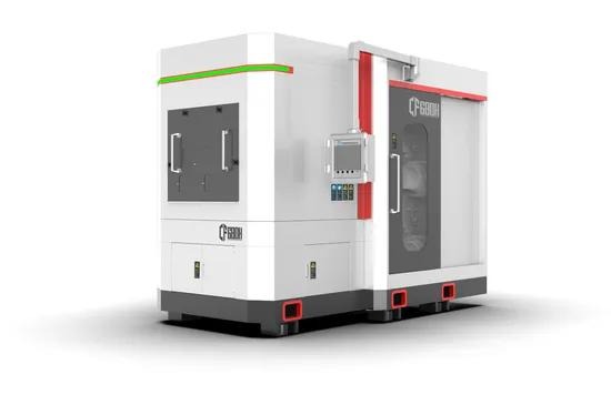 CHIP
Multi-wire saw slicing CZ ingots into wafers with controlled thickness and TTV.
 CHIP
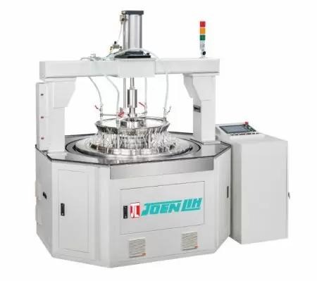
Double-side lapping and CMP-style polish to bring sliced wafers to spec thickness and roughness.
 CHIP
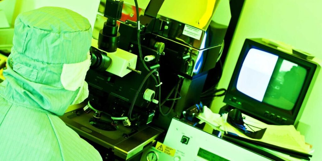
Stepper / scanner exposing wafer resist with DUV or EUV optics for critical layers.
 CHIP
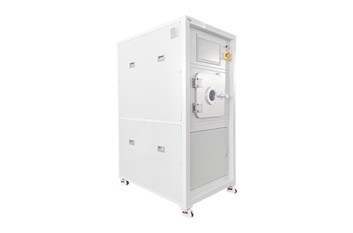
Dry plasma etch for dielectric and metal layers with anisotropic profiles.
Need a panel size, wafer diameter or process window not listed? Send the drawing or process spec — we will source and quote against it.
Capabilities
Drilling, imaging, wet process, lamination and finishing sized to your panel, stack-up and IPC class.
CZ, slicing, polish, lithography, PVD and plasma etch quoted to wafer diameter and process node.
Factory acceptance, utility drawings, spare-parts lists and English operating manuals with the shipment.
Crate packing for precision tools, container loading plans and delivery schedules for line quantities.
Facility & workshop
Process halls and machine bays behind every quotation for PCB and chip equipment.
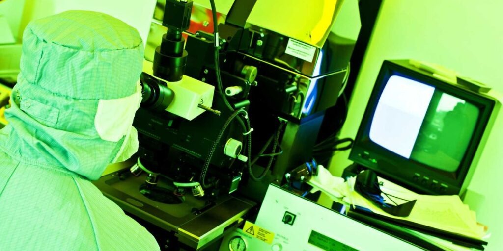
PCB wet lines and wafer tools are quoted as stand-alone machines or as grouped process packages so utilities, layout and spares arrive together.
Quality & documentation
We treat utility drawings, FAT records and spare-parts lists as part of the machine, not paperwork. Process windows are confirmed before dispatch.
HANDOVER PACKAGE
Request a quotation
Tell us PCB or CHIP, panel / wafer size, quantity and destination. The team replies with availability, lead time and a quotation within one business day.